
The tech community remains captivated by the ongoing battle between GPU titans in high-performance computing (HPC), where speed and efficiency are paramount. At the forefront of this fierce competition, NVIDIA’s Tensor Core GPUs have revolutionized the landscape, pushing the boundaries of computational power and opening new horizons for scientific research, artificial intelligence, and data-intensive applications.
In this blog, we delve into the exciting showdown between two prominent NVIDIA GPUs, the A100 and the H100, shedding light on their unique capabilities and exploring the significance of their comparison. These cutting-edge GPUs have redefined what is possible in HPC, leveraging advanced technologies to provide unprecedented performance and scalability.
NVIDIA A100 vs H100 Technical Specs Comparison Table
| Feature | NVIDIA A100 | NVIDIA H100 |
|---|---|---|
| Architecture | Ampere | Hopper |
| CUDA Cores | 6,912 | 18,432 |
| Tensor Cores | 432 (3rd Gen) | 640 (4th Gen) with Transformer Engine |
| Memory | 40 GB / 80 GB HBM2e | 80 GB HBM3 |
| Memory Bandwidth | 2.0 TB/s | 3.35 TB/s |
| FP32 Performance | ~19.5 TFLOPS | ~51 TFLOPS |
| FP8 Performance | Not supported | Over 2,000 TFLOPS |
| NVLink | NVLink 3.0 (600 GB/s) | NVLink 4.0 (900 GB/s) |
| Multi-Instance GPU (MIG) | 1st Gen MIG (up to 7 instances) | 2nd Gen MIG |
| PCIe Power Consumption | ~250W | ~350W |
| SXM Power Consumption | ~400W | ~700W |
NVIDIA A100 Specs and Capabilities
The NVIDIA A100, based on the Ampere architecture, delivers significant advancements over the previous Volta generation. Equipped with 6,912 CUDA cores, 432 third-generation Tensor Cores, and 40 GB or 80 GB of high-bandwidth HBM2e memory, the A100 is engineered for high-performance AI workloads. It offers up to 20× faster performance compared to earlier GPUs in specific mixed-precision tasks.
Benchmark results highlight its strength in deep learning applications, including image recognition, natural language processing (NLP), and speech recognition.
A key innovation in the Ampere architecture is its third-generation Tensor Cores, optimized for high-throughput matrix operations using formats like TF32 and FP16. The A100 also introduces NVIDIA Multi-Instance GPU (MIG) technology, allowing a single GPU to be partitioned into up to seven isolated instances.
NVIDIA H100 Specs and Capabilities
The NVIDIA H100 GPU, built on the Hopper architecture, delivers cutting-edge performance for AI and HPC workloads. It features 18,432 CUDA cores, 640 fourth-generation Tensor Cores, and 80 Streaming Multiprocessors (SMs). The H100 provides up to 51 teraflops of FP32 performance and over 2,000 teraflops using FP8 precision.
It integrates NVLink 4.0 for up to 900 GB/s of GPU-to-GPU bandwidth and supports next-gen workloads like large language models and deep neural networks.
In industry benchmarks like MLPerf, the H100 outperforms the A100 and V100 significantly.
Performance Benchmark Comparison (MLPerf or Workload-Based)
| Workload Type | A100 Performance | H100 Performance | Improvement |
|---|---|---|---|
| BERT Inference | 1× | 3.5–4× | Up to 4× |
| GPT-3 Training | 1× | 2–3× | 2–3× |
| ResNet-50 Training | 1× | 2.2× | 2.2× |
| Scientific Simulation (FP64) | 1× | 2× | 2× |
Architectural Differences Between A100 and H100
The A100 uses HBM2e memory (40/80 GB) with 2.0 TB/s bandwidth. The H100 steps up to HBM3 (80 GB) and 3.35 TB/s bandwidth. H100 includes fourth-gen Tensor Cores and FP8 precision, powered by a Transformer Engine.
Both support MIG, but H100’s 2nd-gen MIG offers better isolation and efficiency.
Power Efficiency Comparison
The H100 GPU draws more power than the A100—up to 700W in SXM form factor versus 400W for the A100. However, this increased power draw is accompanied by significantly improved performance, particularly in workloads optimized for FP8 precision and the Transformer Engine.
When comparing performance-per-watt using standardized benchmarks like MLPerf (e.g., ResNet-50 training), the H100 delivers approximately 60% greater efficiency over the A100. This means that although H100 consumes more energy, it also accomplishes more work per unit of power consumed.
In terms of cooling, the H100 requires more robust thermal management due to its higher power density, but modern data centers are generally equipped to handle this. The efficiency gains justify the added cooling requirements in performance-critical environments.
Best Use Case Scenarios (Table View)
| Use Case Type | Best Choice | Why |
|---|---|---|
| General Deep Learning Training | A100 | Strong performance, cost-effective |
| Large Language Model Training | H100 | FP8 + Transformer Engine, excellent throughput |
| Real-time Inference | H100 | Low-latency, fast memory access |
| Scientific Simulations | H100 | Better FP64 and bandwidth |
| Budget-Conscious AI Projects | A100 | More affordable, widely available |
| Multi-Tenant Environments | Both | H100 has better MIG; A100 is more economical |
Price and Availability Comparison A100 Vs H100
While the H100 clearly outpaces the A100 in terms of raw computational power, it also carries a significantly higher cost—both in terms of hardware resale value and hourly cloud rental rates. To help illustrate the trade-offs between cost and capability, the following visual comparisons break down how the A100 and H100 stack up across three key dimensions: resale market pricing, cloud deployment costs, and normalized AI performance.
As the market shifts toward the Hopper architecture, finding a reliable partner for where to sell used graphics cards like the A100 is crucial for maximizing your budget and funding the transition to more advanced AI infrastructure.
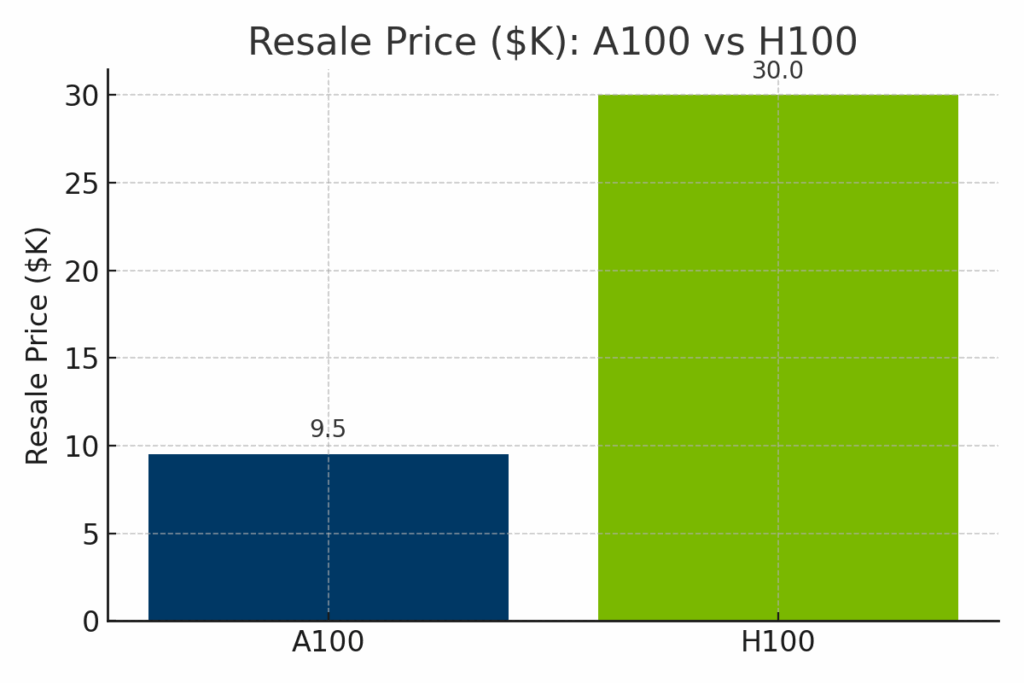
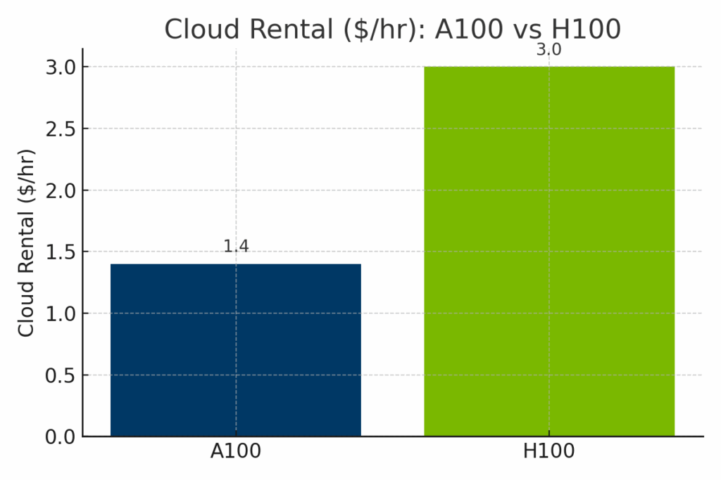
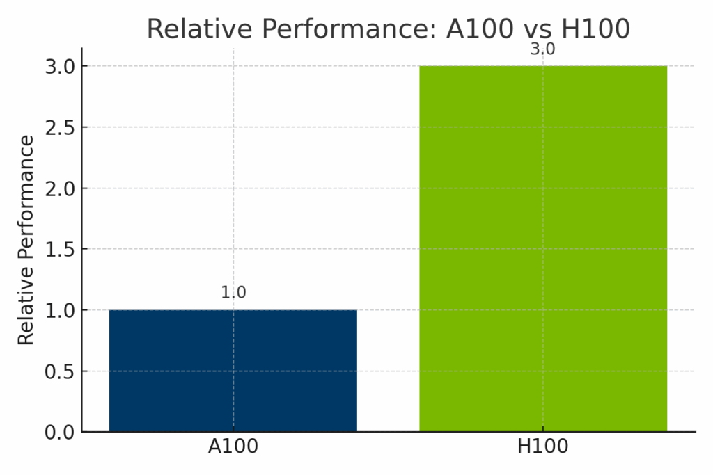
Figure: Estimated resale value of the NVIDIA A100 vs H100 in 2025. The H100 commands a significantly higher resale price—averaging around $30,000—due to its newer architecture and cutting-edge performance, while the A100 typically resells for $9,000–$12,000.
Figure: Hourly cloud rental rates for A100 and H100 GPUs across major providers. H100 instances cost significantly more—often around $3.00/hour—compared to A100’s $1.40/hour average, reflecting the H100’s enhanced AI throughput and newer infrastructure demand.
Figure: Normalized performance of the NVIDIA A100 and H100 across AI workloads. The H100 delivers up to 3× the performance of the A100, especially in transformer-based models and FP8-optimized training, making it ideal for cutting-edge enterprise AI.
NVIDIA Roadmap and Future Developments
NVIDIA’s future graphic cards, based on the upcoming Blackwell architecture (e.g., B100, B200), are expected to provide even greater compute density and memory improvements.
NVIDIA’s software platforms like CUDA, TensorRT, and AI Enterprise are actively maintained to support new workloads.
Software Ecosystem and Developer Support
Both GPUs are supported in CUDA, cuDNN, cuBLAS, TensorRT, and popular frameworks like PyTorch, TensorFlow, and JAX.
H100 benefits from enhanced FP8 support and Transformer Engine optimization within these ecosystems. Developers can use pre-built containers on NVIDIA NGC and robust documentation via the NVIDIA Developer Program.
Pros and Cons Summary
| Category | NVIDIA A100 | NVIDIA H100 |
|---|---|---|
| Pros | Cost-effective, reliable, strong for standard AI/HPC | Best performance, FP8, superior for LLMs and real-time inference |
| Cons | Lacks newer AI features (e.g., FP8, Transformer Engine) | Higher cost, power-intensive, may need infra upgrade |
| Ideal For | Budget-conscious teams, traditional HPC, cloud scaling | Cutting-edge AI workloads, generative AI, enterprise deployments |
Choosing Between A100 and H100 for AI Workloads
Choosing between the A100 and H100 depends on your goals, budget, and use case. A100 is cost-efficient and still powerful for many AI/HPC tasks. H100 is a future-ready powerhouse built for the most demanding workloads.
If you’re upgrading to a newer GPU like the H100, consider selling your legacy hardware to exIT Technologies. Organizations decommissioning GPU-dense servers as part of these upgrades can also sell used servers to recover additional budget. We offer secure and efficient asset recovery services that help you recoup value and responsibly manage your retired infrastructure.
