
The tech community remains captivated by the ongoing battle between GPU titans in high-performance computing (HPC), where speed and efficiency are paramount. At the forefront of this fierce competition, NVIDIA’s Tensor Core GPUs have revolutionized the landscape, pushing the boundaries of computational power and opening new horizons for scientific research, artificial intelligence, and data-intensive applications.
In this blog, we delve into the exciting showdown between two prominent NVIDIA GPUs, the A100 and the H100, shedding light on their unique capabilities and exploring the significance of their comparison. These cutting-edge GPUs have redefined what is possible in HPC, leveraging advanced technologies to provide unprecedented performance and scalability.
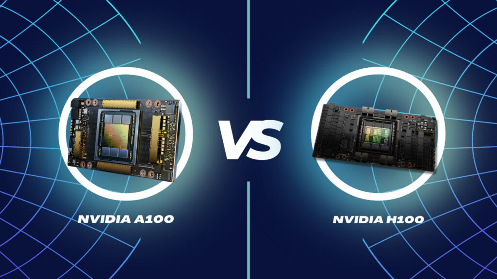
Understanding the NVIDIA A100 GPU
The A100 is built on NVIDIA’s Ampere architecture, which features several improvements over the previous generation’s Volta architecture. It has 6,912 CUDA cores, 432 tensor cores, and 40 GB or 80 GB of high-bandwidth memory (HBM2), which allows it to deliver up to 20 times the performance of its predecessors. In benchmark tests, it has been shown to excel at deep learning workloads such as image recognition, natural language processing, and speech recognition.
One of the key features of the Ampere architecture is its third-generation Tensor Cores, which are designed to accelerate AI workloads by performing matrix operations at higher speeds. In addition, the A100 also includes new hardware for improving data communication between GPUs and CPUs, known as NVIDIA Multi-Instance GPU (MIG) technology.
Exploring the NVIDIA H100 GPU
The H100 GPU features 640 Tensor Cores and 128 RT Cores, providing high-speed processing of complex data sets. It also features 80 Streaming Multiprocessors (SMs) and 18,432 CUDA cores, delivering up to 10.6 teraflops of single-precision performance and 5.3 teraflops of double-precision performance.
The H100 GPU is designed to work seamlessly with NVIDIA’s NVLink interconnect technology, which allows for high-bandwidth communication between GPUs. This enables users to scale up their computing performance quickly and easily, making it an ideal solution for large-scale machine learning and deep learning workloads.
In terms of performance benchmarks, the H100 GPU has been shown to outperform previous-generation NVIDIA GPUs by a wide margin. For example, in a benchmark test using the popular MLPerf benchmark suite, the H100 GPU achieved a performance score of 6,502, more than double that of the previous-generation NVIDIA V100 GPU.
Architecture Comparison: A100 vs H100
One area of comparison that has been drawing attention to NVIDIA’s A100 and H100 is memory architecture and capacity. The A100 boasts an impressive 40GB or 80GB (with A100 80GB) of HBM2 memory, while the H100 falls slightly short with 32GB of HBM2 memory. Another noteworthy difference is that the A100’s Tensor Core improvements over the H100 allow more complex workloads and reduced training times. However, the H100 still holds its ground with a comparable amount of CUDA cores as the A100. Regarding ray tracing capabilities, the A100 and H100 deliver but with different performance levels.
Performance Comparison: A100 vs H100
When it comes to performance, the battle between NVIDIA A100 and H100 rages on. The NVIDIA A100 has built-in features for deep learning purposes that make it stand out from its counterparts. Its Tensor Cores and Multi-Instance GPU technology give it an advantage in processing complex algorithms. For scientific computing, both cards perform quite evenly.
However, the A100’s high memory bandwidth and terabyte-sized cache make it a top contender for data-heavy tasks. Regarding gaming, the H100 may have a slight edge over the A100. Its lower power consumption and faster clock speeds may translate into faster, smoother gameplay.
Power Efficiency: A100 vs H100
When it comes to power efficiency in GPUs, both cards are known for their impressive features and capabilities; it’s their power consumption where the greatest differences lie. The A100 runs on a minor power of 400 watts and even goes as low as 250 watts on some workloads. On the other hand, the H100 is known for its higher power consumption which goes up to 500 watts in some scenarios. However, these differences go beyond just the numbers, as the A100’s lower power consumption means it’s more energy-efficient overall.
Use Cases and Applications
When it comes to the NVIDIA A100 and H100, various use cases and applications cater to specific needs. The A100 is designed for high-performance computing and is perfect for complex data modeling and neural network training. On the other hand, the H100 is more geared towards scientific research and simulations, making it ideal for data-intensive workloads such as astrophysics and climate modeling. Both GPUs have their benefits when it comes to data centers and cloud computing. The A100 is optimized for multi-node scaling, while the H100 provides high-speed interconnects for workload acceleration.
Price and Availability
While the A100 is priced in a higher range, its superior performance and capabilities may make it worth the investment for those who need its power. On the other hand, the H100 provides a more affordable option for individuals who may not need such top-of-the-line features. Availability and market demand also play a significant role in pricing these GPUs, with regular fluctuations occurring.
Future Developments and Roadmap
NVIDIA has been a prominent player in the GPU industry, continuously pushing the boundaries of technology. The latest A100 and H100 GPUs have been game-changers, delivering massive improvements in performance and efficiency. The company’s roadmap suggests the next generation will bring even more enhancements and advancements. We can expect improvements in AI, gaming, and data center operations. The company invests heavily in research and development to ensure that future GPUs will be even more powerful and versatile than their predecessors.
Comparing Support and Software
When it comes to NVIDIA’s A100 and H100 graphics cards, the software ecosystem and developer support can make all the difference. Fortunately, NVIDIA has a strong track record of providing excellent support and robust software for its products. So whether you’re a developer looking to tap into the full potential of your NVIDIA card or simply a user trying to get the most out of your investment, you’ll find plenty of resources and assistance available.
And with a vibrant community of developers and users constantly pushing the boundaries of what’s possible with NVIDIA’s technology, the future looks bright for anyone looking to explore the possibilities of this powerful hardware.
Pros and Cons: A100 vs H100
The A100 is designed for data centers and boasts impressive AI and machine learning capabilities. Its advantages include faster performance, increased memory capacity, and improved energy efficiency. However, its advanced features come at a higher cost than the H100.
On the other hand, the H100 is more budget-friendly and an excellent option for gamers and casual users. Its advantages lie in its compatibility with various operating systems, ease of integration into existing systems, and superior streaming capabilities. However, its processing speed may be slower than the A100, which can be a drawback for those looking for lightning-fast graphics.
A100 vs H100: Which GPU is Right for You?
When it comes to choosing between the A100 and H100 GPU, it can be a challenging decision. There are a few factors to consider, such as your use-case scenario and budget. The A100 is a more powerful GPU ideal for intensive AI tasks such as deep learning, simulation, and analytics. If you plan on using your GPU for machine learning or big data processing, the A100 is the way to go.
On the other hand, the H100 is more suitable for graphics-intensive tasks like gaming and professional graphics work. It’s also more affordable and offers good value for money. Ultimately, the choice comes down to your specific needs, and we recommend taking a closer look at your use case scenarios before making a final decision.
Frequently Asked Questions (FAQs)
Q: Can the A100 and H100 be used interchangeably?
A: The A100 and H100 GPUs cannot be used interchangeably. They have different form factors and are designed for different use cases.
Q: What are the key differences between A100 and H100 regarding performance?
A: The A100 is designed for high-performance computing (HPC) and artificial intelligence (AI) workloads, while the H100 is designed for graphics-intensive workloads. The A100 has a higher memory bandwidth, more Tensor Cores, and supports larger models than the H100.
Q: How do the A100 and H100 GPUs compare in price?
A: The A100 is more expensive than the H100 due to its higher performance and advanced features. The exact price difference varies depending on the vendor and specific configuration.
Q: Which industries can benefit the most from A100 and H100 GPUs?
A: Industries that require high-performance computing and AI capabilities can benefit from the A100, including healthcare, finance, and scientific research. Industries that rely on graphics-intensive workloads, such as media and entertainment, can benefit from the H100.
Conclusion
It’s been a true battle of the titans as NVIDIA’s latest GPU release, the A100, makes its way onto the market and directly faces off against the popular H100. Gamers and tech enthusiasts alike are itching to get their hands on these highly coveted pieces of hardware, as both offer significant improvements in processing and speed over previous GPU models. But with so much hype and competition, it’s important to remember that these upgrades come at a cost.
So if you want to upgrade your graphics processing power, why not sell your old gear to Exit Technologies? It’s a great way to save cash and give your old technology a second life.